From the research on transparent organic light-emitting diodes with balanced white emission by minimizing waveguide and surface plasmonic loss by YI-BO ZHANG,1 QING-DONG OU,1 YAN-QING LI,1 JING-DE CHEN,1 XINDONG ZHAO,1 JIAN WEI,1 ZHONG-ZHI XIE,1 AND JIAN-XIN TANG1,2,*,
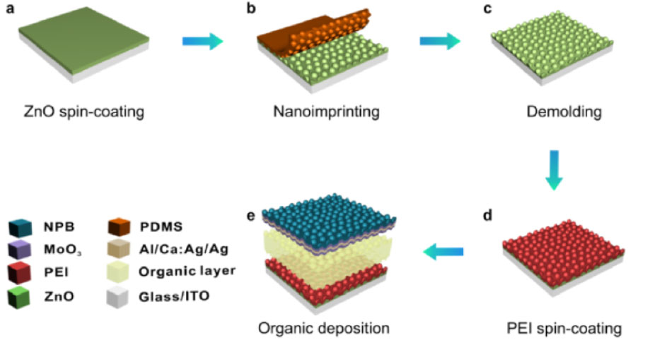
Following steps:
(a) Spin-coating the ZnO layer on ITO-glass substrate.
(b) Imprinting the ZnO layer with the PDMS mold.
(c) Demolding the PDMS mold.
(d) Spin-coating the PEI interlayer on the patterned ZnO layer.
(e) Depositing the organic layers and MDCE multilayer onto the patterned PEI/ZnO layer.
The ZnO precursor solution spin coated on cleaned-ITO glass substrate at 4000 rpm for 40 s and then annealed in ambient air at 150 °C for 30 s.
An about 4 nm thick polyethyleneimine (PEI) layer was spin-coated onto the ZnO layer from a 2-methoxyethanol solution (0.4 wt.%) at 5000 rpm for 50 s, and then was annealed at 100 °C for 10 min in ambient air.

Fig. 1. Schematic illustration of the fabrication process of nanostructured white transparent OLEDs
Source: Transparent organic light-emitting diodes with balanced white emission by minimizing waveguide and surface plasmonic loss YI-BO ZHANG,1 QING-DONG OU,1 YAN-QING LI,1 JING-DE CHEN,1 XINDONG ZHAO,1 JIAN WEI,1 ZHONG-ZHI XIE,1 AND JIAN-XIN TANG1,2,* 1Institute of Functional Nano & Soft Materials (FUNSOM), Jiangsu Key Laboratory for Carbon-Based Functional Materials & Devices, Soochow University, Suzhou 215123, China 2Institute of Organic Optoelectronics (IOO), JITRI, Wujiang, Suzhou, China *jxtang@suda.edu.cn


